Our Research
Low-dimensional materials have been the subject of fundamental research because of their unique characteristics arising from reduced degrees of freedom and enhanced correlation effects. The response of these systems towards the external perturbations and lattice irregularities like applied field, strain, doping, dislocations etc. gives birth to many exciting properties which have been attracting the scientific explorations over decades. It has been of escalating interest from technological point of view as well in this era of miniaturized devices. The urge of fundamental understanding of the material behaviors in presence of quantum confinement along with the promising application possibilities has driven us to study some of the intriguing phenomena in low-dimensional and nanoscale materials with special emphasize on graphene and other two-dimensional materials.
Click on the following topics for more details
► Graphene and Graphene Nanoribbons (GNRs):
Graphene has made possible the understanding of various properties for the first time in truly two-dimension and has opened up huge possibilities in future applications in nanoelectronics and devices because of its very high charge carrier mobilities. It exhibits many exotic phenomena like unusual quantum Hall effect, breakdown of adiabatic Born-Oppenheimer approximation, Klein paradox, exotic superconductivity, metal free magnetism, ballistic electronic propagation etc. owing to the peculiar behavior of its charge carriers and unique band structure.
The charge carriers in graphene are mostly described as massless relativistic Dirac fermions. The hexagonal Brillouin zone consists of two inequivalent k points, namely K and K’, known as Dirac points where the bands from two different sublattices intersect to give rise to conical dispersion for the two dimensional bipartite graphene lattice. Strong nanoscale and edge effects on its electronic and magnetic properties make it an interesting material for device applications. Depending on the direction of crystal termination, GNRs can show two different edge geometries, e.g., zigzag and armchair with distinct electronic properties arising from different boundary conditions. All these features have made graphene and its analogues the ideal material for 21st century research in both experimental and theoretical materials science research.
Click on the following topics for more details
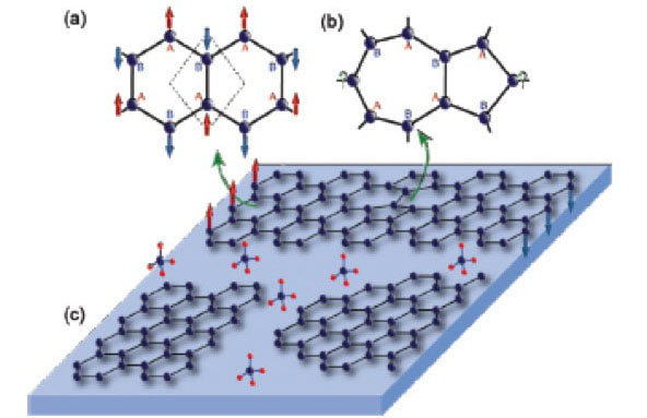
Introduction of magnetism in graphene in terms of defects has been gaining interest in recent times, owing to their application possibilities towards spin transport and sensor devices. The fundamental concept of magnetism in graphene bipartite lattice lies in Lieb’s theorem, which says: the inequality between two sublattice points, A and B (see Fig.1a and Fig.1b) introduces net magnetic moment. The graphene unitcell consists of two sublattice points, A and B that prefer opposite spin occupancies, making the over all net magnetization zero (see Fig.1a). Therefore, the vacancy defects can introduce inequality between A and B, making the two-dimensional graphene magnetic.
The magnetism in graphene can also arise from the point boundaries induce dispersion less flat bands near Fermi energy, showing higher localization of electrons. These flat bands can be accessed via small doping, leading to enhanced magnetism. Moreover, net magnetization in graphene can induce asymmetric spin conduction behavior across the magnetic grain boundaries. Our study shows for the first time that, the grain boundaries in graphene can be exploited for spin-filtering applications.
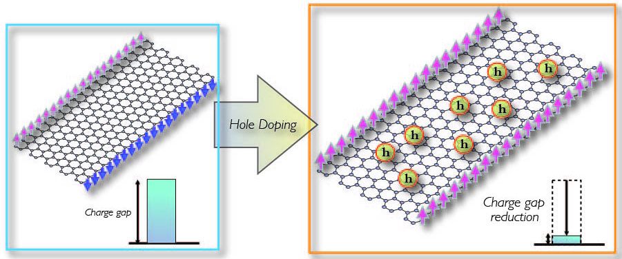
The formation of zigzag edges, a defect, introduced by finite termination of graphene along a certain crystallographic direction can also introduce net magnetization (see Fig.1c). This observation of carbon-based magnetism motivates the fabrication of spintronics devices using graphene nanoribbons. It requires the knowledge of the interplay between the edge magnetism and hole-doping effect since the electron density in graphene system can be easily tuned using the back gate electrode. However, the hole doping effect on edge magnetism with proper inclusion of electron-electron interactions has not been studied.
In view of this, we have modeled the zigzag edge GNRs (ZGNRs) within Hubbard Hamiltonian and have developed many-body configuration interaction (CI) based numerical technique to investigate their magnetic and conducting properties and their response to the hole doping. For half-filled case, the many body ground state shows the ferromagnetic spin-spin correlation along the zigzag edge, which is consistent with the picture obtained from one-electron theory. The charge gap shows minima near Dirac point. However, investigation on spin gap reveals gap-less spin excitation, an indication of magnetic ground state over the flat band, i.e., the edge localized states. The microscopic origin of magnetism in ZGNRs can be well understood on the basis of a generic two-state model. We further observe that, the enhanced electronic correlation in other honeycomb ribbons like silicene, dichalcogenides, molecular graphenes and Fermionic optical lattices produces insulating and magnetic ground states. The combination of these two properties can convert the electrical signals into spin-wave which can propagate over longer distance compared to normal conduction electrons, as has been observed recently in case of garnet compounds. This behavior can find huge applications in spintronics as spin-wave spin-transport.
We observe hole mediated metallic ferromagnetism that can be exploited to realize the magneto-transport devices (see Fig.2). Consistent observations of charge and spin gap properties for finite size graphene quantum dot structures with long zigzag edges indicate that, the effect of scattering processes connecting different momentum also lead to similar conclusions.
The many-body configuration interaction (CI) method gives good estimation of excited states along with the ground state, enabling the study of spectroscopic properties of strongly correlated systems. We have modeled the armchair and zigzag edge GNRs within Hubbard and extended Hubbard Hamiltonian to study their electronic and spectroscopic properties. The ground state of zigzag GNRs shows high spin state, whereas the armchair GNRs exhibit singlet behavior. However, in both the cases, the low-lying excitations are magnetic. Analysis of optical states suggests differences in quantum efficiency of luminescence for zigzag and armchair GNRs, which can be probed by simple experiments. Our study suggests an alternative way of detecting the edge geometry of graphene.
The quest for novel functionalities has driven us to investigate the GNRs further with various geometrical and chemical modifications. Our investigations within first-principle calculations reveal that, the anti-ferromagnetic ground state of edge passivated (with hydrogen) ZGNRs exhibits half-metallic behavior beyond a certain electric field along the cross-ribbon direction within both local and semi-local exchange correlations approximations. Moreover, the doping of both the edges of ZGNRs with boron atoms stabilizes the system in a ferromagnetic and half-metallic ground state.
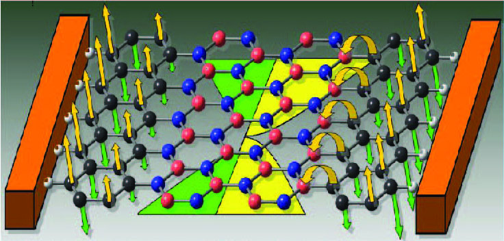
The chemical modifications of ZGNRs with simultaneous boron and nitrogen substitution, keeping the whole system isoelectronic stabilize the systems in antiferromagnetic ground states. The concentrations and positions of substituents regulate the electronic structure of the nanoribbons, exhibiting both semiconducting and half-metallic behaviors as a response to the external electric field. Interestingly, our study shows that zigzag boron nitride nanoribbon with terminating polyacene units exhibit half-metallicity irrespective of the ribbon width as well as applied electric field. We have exploited the basic knowledge of Lewis acid/base characteristics of boron/nitrogen atoms for the first time to set up the potential gradient across the ribbon width, making the ribbons intrinsically half-metal (see Fig.3).
► Atomic sheets beyond Graphene:
The lack of band-gap in graphene puts severe limitations for its applications in semiconductor industry. This fact motivated the search for other 2D materials with promising electronic properties in recent times. This family of materials allows the fabrication of single-layer or a few-layer samples using mechanical cleavage or chemical exfoliation techniques, owing to their layered structures resembling graphite. In addition, atomically thin films can be grown on substrates using the bottom-up epitaxial techniques. These atomic sheets are very sensitive towards structural and chemical modifications giving rise to new functionalities, which can be exploited for the electronic and opto-electronic applications.
Click on the following topics for more details
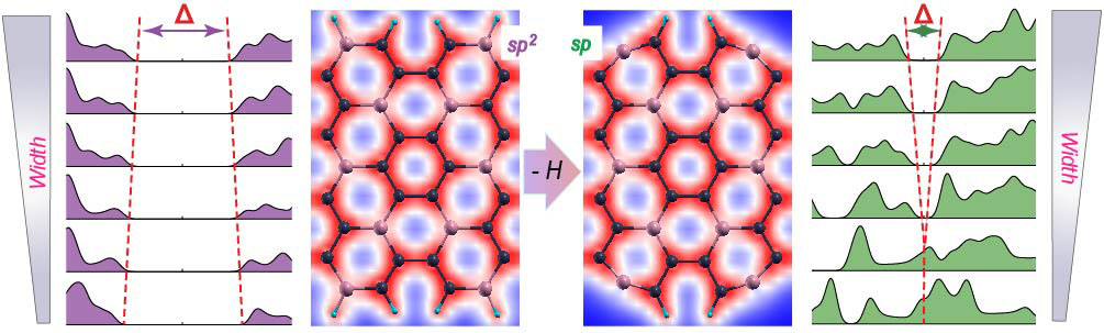
One such atomically thin material is BC3, an indirect gap semiconductor with each boron atom connecting three separate carbon hexagons. Ab-initio calculations on armchair BC3 ribbons show that, the removal of passivating hydrogen from the edge boron atoms provides higher stability and makes the narrower ribbons metallic due to the enhanced p-conjugation along the edge. However, an increase in the ribbon width results in an unprecedented metal-to-semiconductor transition, as can be seen from the density of states plot in Fig.4. In case of semiconducting zigzag ribbons, the removal of passivating hydrogen atoms from edge boron atoms produces robust edge states at Fermi energy and consequent metallicity which does not change upon increase in width. Our study shows the importance of edge passivation to regulate the electronic properties of atomic sheets.
► Transition Metal Dichalcogenides
Our recent studies with experimental collaboration shows the self-limiting layer-by-layer oxidation of WSe2 system in presence of ozone. The ozone oxidizes the top layer producing an amorphous composite at a certain temperature, which protects the underlying layers from further oxidation. The oxidation of subsequent layers takes place only at elevated temperature. Our theoretical investigations reveal the oxidation mechanism of this layered material and shows that the oxidized top layers inject holes to the underlying WSe2 layers. As a result, the semiconducting WSe2 systems become metallic.
► Intercalated Layered Materials:
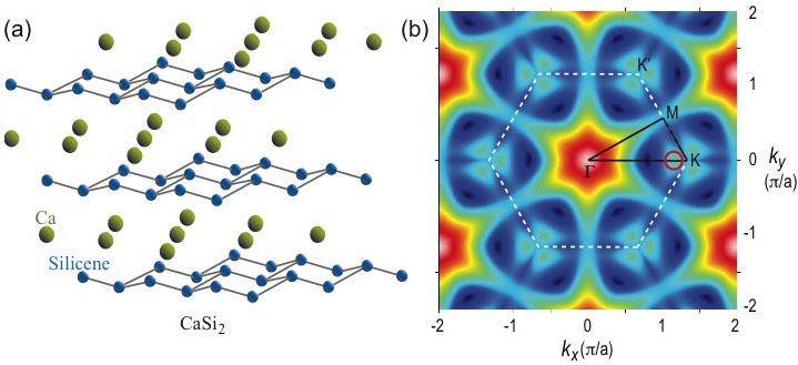
The intercalated graphitic compounds are of sustained interest due to their unusual superconducting properties. Recently the Ca intercalated silicene compound, CaSi2 (see Fig.5(a)) is reported due to their interesting Dirac electron behavior. Our theoretical investigation within ab-initio level of theory, shows that the Dirac cone shifts from the high-symmetric points K and K’ of the hexagonal Brillouin zone (Fig.5b) due to the interlayer interactions and sublattice symmetry breaking invoked by the buckled geometry of silicene. Our observations can provide the guideline to the escalating research on this class of materials.
► Quantum Phase Transitions in Strongly Correlated Systems:
We too have explored the rich phase diagram of strongly correlated one- dimensional systems as a response to the static and dynamic external electric field within many-body framework. The density matrix renormalization group (DMRG) technique has been adopted to study one-dimensional Mott and Peierls chains, modeled within Peierls-Hubbard Hamiltonian. The electric field induces multiple negative differential resistance (NDR) for finite-size systems. To investigate the quantum dynamics of insulating rings described by extended Hubbard Hamiltonian in non-equilibrium situation, we have developed a combined approach of exact-diagonalization and Cranck-Nicholson algorithm. The inclusion of time-dependent electric field as Aharonov-Bohm flux makes the hopping term time-dependent. The behavior of current density and average current as a response to the applied field suggest a dielectric breakdown of both charge-density-wave (CDW) and spin-density-wave (SDW) phases beyond a certain field strength, which is further confirmed by the Tomonaga-Luttinger liquid order parameter. The CDW phase undergoes a field mediated phase transition to insulating SDW phase before the dielectric breakdown, which is confirmed by the nature of the correlation length and the behavior of the order parameter calculated in terms of charge and spin structure factors. This indicates the field-induced charge ordering of the insulating phases.